Assignment 2 Answers
Q2.1
I observe noise with a peak-to-peak amplitude ~20 mV. The noise is mostly a 60 Hz oscillation.
I can increase the noise to over 200 mV by bringing my hands close to the cable and/or touching it.
The nature of this noise will likely differ for each of you.
Q2.2
We’re interested in the amplitude of the current induced in our antenna. We know that the current is flowing across a resistance of ~1 MΩ to generate the voltage noise. Let’s use a round number of ~100 mV for the noise amplitude. By Ohm’s law:
$ I = \frac{V}{R} = \frac{0.1 \mathrm{V}}{1,000,000 \mathrm{ Ω}} = 0.1 \mathrm{ µA}. $
Q2.3
(a) Switching from a ~2 m ribbon cable to a 6” jumper reduced the peak-to-peak noise from ~20 mV to ~6 mV.
(b) Adding shielding reduced the noise to ~4 mV, and grounding the shield brought it down to under 1 mV. Furthermore, with the grounded shield the noise didn’t increase when I approached or touched the shield.
Q2.4
In order to filer out the high frequency band, I used a low-pass RC filter. Conversely, I used a high-pass RC filter to remove the slow 5 Hz sine. My circuits looked just like those from Assignment 1, section 3.1.
To determine reasonable values for $R$ and $C$, you could use your empirical results from Q1.4. I decided to be a bit more quantitative and used the formula for cut-off frequency in the slides from lecture 1: $ f_{c} = 1/(2 \pi RC) $, where $f_c$ is the cut-off frequency in Hz. Because RC filters have a shallow cut-off, I aimed for a $f_c$ midway between 50 Hz and 1 kHz (on a logarithmic scale). I arrived at $C$ = 0.1µF and $R$ = 10 kΩ, which should result in $f_c$ = ~160 Hz.
Q2.5
We can apply the voltage divider equation to determine $V_F$:
$V_F=\frac{R_1}{R_1+R_F}*V_{Out}$
Given that $V_F=V_{In}$ due to Op Amp feedback:
$V_{In}=\frac{R_1}{R_1+R_F}*V_{Out}$
And finally, gain is the ratio of output to input, which simplifies to:
$G_V=\frac{V_{Out}}{V_{In}}=1+\frac{R_F}{R_1}$
Q2.6
Setting $R_F$ and $R_1$ to identical value will result in gain = 2. I chose, 50.5 kΩ for both resistors. With the values chosen, I measured the input waveform at 5 V and the output at 10 V.
Q2.7
As gain is increased, the output waveform starts to clip. This happens because the Op Amp is limited by its voltage supply rails.
Q2.8
Gain for the inverting amplifier is given by $G_V=-\frac{R_F}{R_{In}}$. I chose $R_{In}=\mathrm{1 k\Omega}$ and $R_F=\mathrm{9.8 k\Omega}$
Q2.9
The input impedance for this circuit is $R_{In}$, which is 1 kΩ for the values chosen above. Compare this to the input impedance of the Op Amp terminal, which ranges from 100s MΩ to several GΩ. With a 1 V source, by Ohm’s Law, the circuit would draw up to 1 mA into its input impedance. This may seem like a small amount, but it’s more than many sources can output.
Q2.10
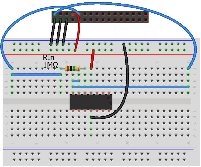
Below is the wiring diagram that shows the buffer and the 1 MΩ resistor that models our high impedance source.

(a) With the buffer in place, the correct 1 V waveform is measured because the input impedance of the buffer is much greater than the 1 MΩ signal source impedance.
(b) Once we connect the oscilloscope to the buffer input, we once again degrade the waveform. The measured waveform is approximately .5 V because the input impedance of the oscilloscope probe makes a voltage divider with the source impedance of the circuit. The buffer output shows the same .5 V waveform
Q2.11
I chose 51k and 10k for Rf and R1, respectively. The calculated voltage gain is 6.1
Q2.12
Because the input signal is zero-centered, and the amplifier only has a positive power supply, the output waveform only shows positive values. The circuit is unable to amplify the negative portion of the signal.