Assignment 3: Digitization
Digitizing an analog voltage signal converts it into discrete steps of voltage and time. This is necessary to digitally manipulate the signal, to store it in digital media (hard drive or flash memory), and to display it on a monitor. In sections 1 and 2 of this assignment we will consider issues related to digitizing the voltage scale and in sections 3, 4, and 5 we will explore the time axis.
1. Bit noise and dynamic range
The oscilloscope inputs on the Analog Discovery can measure signals up to ±25 V — this is called its Dynamic Range. On the AD, and on every acquisition system, the full voltage range is subdivided into steps, and the total number of steps is equal to $\mathrm{2^{n}}$, where n is the number of digitizer bits. For example, a 10-bit digitizer would partition the full input voltage range into 1024 equal segments.
Q3.1 The AD uses a 14-bit digitizer on its oscilloscope channels. When looking at small signals, the AD reduces its dynamic range to 5 V. What is the smallest theoretical voltage step that the AD can record?
The discrete nature of the digitized signal means that there will be a discrepancy between the true analog waveform and the digitally sampled one. This error is called bit noise or quantization noise.
To minimize the relative error due to bit noise, you should amplify the signal to fill most of the dynamic range before digitizing with your acquisition system. Alternatively, if the acquisition system allows it, you should set the dynamic range to be slightly larger than the biggest signal you expect to record.
2. AC Coupling
As we saw in class, sometimes a signal of interest rides on top of a (slowly drifting) voltage offset. If such a signal were digitized directly, the slowly varying drift can take up most of the digitizer’s dynamic range. Merely amplifying the full signal would amplify the offset too, so it is sometimes beneficial to filter out this low-frequency component to isolate the small signal of interest. An input device that performs this filtering is called AC coupled, in contrast to a DC coupled input that accepts the low frequencies.
For this assignment you will start by generating a small “spike train” signal superimposed on a slowly changing offset. Open the Wavegen tab and select Play from the dropdown menu currently labeled “Simple”. Download the “SpikesWithDrift” waveform file and use the Import button to load it up and generate it on W1. Finally, specify Frequency: 5 kHz and Amplitude: 2 V. Observe the waveform on O1 — it should resemble small “spikes” riding on a drifting baseline.
The Op Amp circuit shown below has an input capacitor that blocks DC signals. You can think of the input RC pair as a high-pass filter. Build this circuit on the breadboard. Use $R_F = 10 \mathrm{k} \Omega$, $R_1 = 4.7 \mathrm{k} \Omega$, and $C = 1 \mathrm{\mu} F$ (this is the larger of the two capacitors that we gave you). Note that other than the input capacitor, the circuit looks just like the inverting amplifier we saw in lecture 2. The gain for this ampifier is $G_v=-\frac{R_f}{R_1}$ and at high frequencies, the capacitor “looks” like a short circuit and the gain is -2. At low frequencies, the gain of this circuit approaches zero.
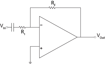
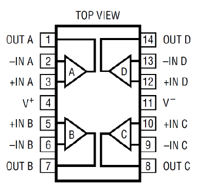
Because this signal has positive and negative values, we need to provide the Op Amp with both positive and negative power supplies. If you previously wired pin 11 of the Op Amp to ground, remove that connection, and instead connect pin 11 to the negative supply rail on the black header of the AD (refer to the figure Op Amp Power Connections in assignment 2 to help you identify the negative supply pin). Wire pin 4 to the positive supply rail. Connect O1 to the input and O2 to the output. If these connections are confusing, you can take a peek at the answer key for help.
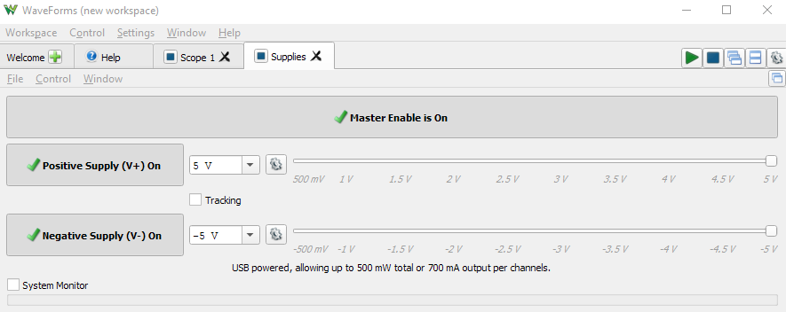
To power the Op Amp from the Analog Discovery, go to the Welcome tab and select Supplies. This will present a new tab, which has two supplies available. Set one supply to 5V and the other to -5V, enable them and turn them on by clicking the appropriate buttons, as shown below.
Q3.2 Connect the “spikes with drift” waveform to this AC-coupled amplifier. Plot the W1 waveform on O1 and plot the output of the amplifier on O2. Describe the output waveform. Is the drift completely gone, and if not, why not?
To better understand the frequency dependent behavior of this circuit, we can look at its response across a range of frequencies. In the Welcome tab, select Network to create a new tab. From the bar across the top, select Start: 5 Hz, Stop: 1 MHz, Steps: 51, and set Amplitude: 200 mV. On the right panel (still within the Network tab) in the Magnitude window, select units: gain(X) and set the range from 0 X to 5 X. In the Phase window set Ref: Channel 2. Execute the frequency sweep by pressing the Run button on the top bar. You might need to wait several seconds before the results start to appear. The output that results is called a Bode Plot, and it shows the magnitude and phase response of the system to a frequency sweep.
If the measurement happened correctly, the magnitude window should display a hump around a few kHz. This magnitude response represents the gain of the AC-coupled Op Amp circuit. The gain is small at low frequencies, then it grows as we move into the passband of the RC filter, and eventually the gain drops off again as the Op Amp is no longer able to keep up with the signal.
Q3.3 From your Bode Plot read off the maximum amplification of the circuit.
3. Aliasing
Digital oscilloscopes typically sample their incoming signals at very high frequencies. For example, the Analog Discovery acquires 100 million samples per second (100 MHz). On the other hand, most digitization in biology labs occurs at lower sampling rates: typically 100 kHz, or even much slower. (For instance, if the fastest events you want to measure have a time scale of ~1 ms, then you may not need to acquire data faster than a few 10s of kHz.) Collecting data at a higher rate is not only unnecessary, but will increase data storage needs (e.g., disk space) and analysis time.
For the remainder of this assignment, we will simulate a device that samples data at a rate of 10 kHz. To do this, we must disable some features of the Analog Discovery that take advantage of its higher sampling rate:
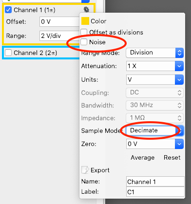
In the Scope tab, open up the Channel 1 gear menu (see figure). Deselect the Noise checkbox, and select Sample Mode: Decimate.
Next open up the extended time settings panel by pressing the green down arrow below the time scale adjustments (see figure). Adjust Rate to 10 kHz, and Samples to 100.
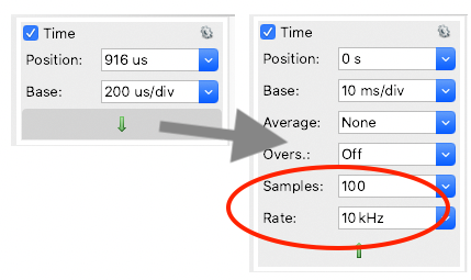
With these settings in place, the oscilloscope is sampling the input voltage at 10 kHz (i.e., ten times a millisecond) and displaying each sampled value on the screen (connected by line segments). NOTE: If you change the time scale (by zooming in or out), you may undo these settings and have to repeat the steps above.
Generate a 1 kHz sine wave on W1 and record it in the oscilloscope without changing the time scale settings. (Do adjust the voltage scale as needed.) Convince yourself that the waveform displayed by the scope does, in fact, have a 1 kHz frequency by noting that the duration of each cycle is 1 ms.
You can also enable a frequency domain display by selecting the FFT button in the top toolbar. (FFT stands for Fast Fourier Transform.) The FFT plot should also indicate that the peak frequency component is 1 kHz.
Q3.4a Now slowly increase the frequency on W1 from 1 to 15 kHz in steps of 1 kHz. Can you describe (briefly) what happens and why?
Q3.4b Next, test whether aliasing can be a problem even when the signal frequency is orders of magnitude larger than the sampling rate. E.g., try with 1001 kHz. Does aliasing still occur?
Just for fun, try observing the aliasing artifact at 5.05 kHz.
4. Anti-aliasing filters
The previous section demonstrated the subtle and sneaky nature of aliasing artifacts. If you are sampling at 10 kHz, any noise (or even signal) with frequencies above 5 kHz will still contribute to the signal you record. Moreover, even signals between ~3–5 kHz can be significantly degraded. The problem is that you have no way to detect that these are aliasing artifacts. An input sine wave of 8 kHz, when acquired at 10 kHz, will look identical to an input wave of 2 kHz. Once acquired there is no general way to detect and filter out these fictitious signals with an algorithm or software filter. Thus, the best way to avoid aliasing problems is by filtering out high frequencies before acquisition, using a hardware filter.
Q3.5 Given that you are acquiring at 10 kHz, how should you filter the input signal to reduce or eliminate the frequencies that would get aliased? (High-pass or low-pass filter? What should the cut-off frequency be?)
Q3.6 The simple RC filters you’ve built in this course do not have sharp frequency cut-offs. Nevertheless, implement an RC filter based on on your recommendation from Q3.5 (and working with your limited set of components). Repeat the sine wave presentation from Q3.4: How well does your filter attenuate the frequencies that cause aliasing?
5. Using an oscilloscope to measure timing and jitter
In experimental rigs, we often want to generate precisely timed stimuli (laser pulses, water valve opening, light flashes, etc). Unfortunately, the software running on a standard PC is unsuitable for directly generating timing signals. Because the computer is multi-tasking (running the operating system, handling network requests, etc.), you typically cannot control the timing of software commands with a precision of milliseconds. On the other hand, dedicated hardware — like the AD or a DAQ card — are perfectly suited to generating precise timing. This question will demonstrate this distinction, and will provide an opportunity to use your oscilloscope to measure durations, offset, and jitter.
Download this Waveforms workspace and open it in Waveforms (Workspace menu -> Open). Next, wire up your breadboard as shown below, so that the signal from W1 goes to O1 and to the AD port marked T1 (Trigger-1). The signal from W2 should be wired to O2.
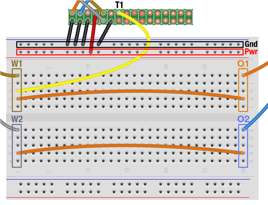
Once your breadboard is wired up, go to the Script subwindow and press Run. This should generate a continuous train of 100 ms long pulses on W1 and W2. The durtion of the pulses on W1 are controlled by the script running on your computer (within Waveforms). The script initiates a pulse, waits 100 ms, and then ends it. It then repeats this process once per second.
In contrast, the pulse durations on W2 are hardware controlled. The AD hardware is triggered to generate a pulse on W2 every time it detects new pulses on W1. The W2 pulses use hardware timing to ensure a 100 ms duration.
Q3.7 Use the oscilloscope to measure duration of software timed pulse on W1. Can you estimate the mean duration as well as the amount of jitter? (Hint, trigger on the rising edge of the pulse, but zoom in on the falling edge (the end) of the pulse (try 500µs/division). Then use the Persistence tab to observe pulse-to-pulse jitter.)
Q3.8 Now look at the hardware controlled pulse on W2. This pulse is triggered by the onset of the pulse on W1. What is the time delay between the onset of the pulses on the two channels (this is the time it takes for the h/w to detect the trigger and initiate a new pulse)? What is the duration (mean & jitter) of the h/w controlled pulse?
For situations where millisecond timing matters (e.g., optogenetic stimulation, behavioral control), you can see why it’s important to (a) use hardware timing whenever possible, and (b) measure the timing in your system (timing offsets, durations, jitter) to confirm that it operates as you intend.
Parts List
Parts from Assignments 1 & 2, plus:
- 1.0 µF capacitor