Assignment 2: Noise, Filtering, and Amplifiers
In this assignment we will ask you to measure the noise in various circuits. Note that the conditions that cause noise differ from one location to another and are hard to control so the behavior of your noise will likely differ from your classmates and from what the instructors experienced when writing this assignment.
1. EM Pickup Noise
One common form of noise in lab equipment is EM (electromagnetic) pickup. Any unshielded wire acts as an antenna, picking up electromagnetic radiation in the environment and converting it into small currents in the wire. These currents, in turn, can generate unwanted voltage fluctuations in high-impedance lines.
1.1 Measure EM pickup on a high-impedance line
In assignment 1 we simulated a high-impedance source, like a neuron, by recording the signal generated by W1 when followed by a 1 MΩ resistor. Set up the same circuit from assignment 1, section 2.3, but this time increase the length of the measurement line by sending the high-impedance signal over the ribbon cable (use pin 1) before connecting to the oscilloscope. To make things simple, generate a constant 0 V signal by selecting Type: DC and Offset: 0V in the Wavegen tab. Now, use the oscilloscope to observe the noise level. You may need to adjust the voltage scale to make the noise visible.
Q2.1 What is the amplitude of the noise that you observe? Do you notice any structure to it (e.g., is there an oscillation at a particular frequency)? Can you do anything to change the nature of the noise? (Try moving the cable around or bringing objects (your hands, something metal, something electronic?) near it.)
Q2.2 Can you estimate the magnitude of the noise currents (in Amps)? (Use Ohm’s law and consider that the current is flowing across the 1 MΩ resistor.)
1.2 Reducing EM pickup
Reducing EM pickup is often challenging, but fortunately, there are several strategies for doing so:
-
Eliminate sources of EM radiation. Unfortunately EM radiation is ubiquitous in the modern lab environment, generated by fluctuating electric currents in nearby equipment and power lines. You might be able to move your rig away from a particularly strong EM emitter, but you’re unlikely to escape all EM noise.
-
Decrease the length of your antenna. The length and geometry of an antenna determine the amplitude and bandwidth of EM pickup. On average, a shorter antenna will pick up less noise. Thus, you can reduce noise by minimizing the length of any high-impedance lines.
Q2.3a To demonstrate this, replace the long ribbon cable with the standard 6 inch jumper wire. How does the noise level change?
-
Shielding. A grounded conductive shield can be used to attenuate EM waves, or even block them completely. In a typical rig, you will find shields in the form of: Faraday cages, shielded wires (coaxial cables like BNC or SMA), and the metal box surrounding electronic instruments. It is often possible to shield sensitive wires or rig components by (a) placing them in a Faraday cage (a large enclosure made from wire mesh or solid metal panels), or (b) wrapping them in conductive foil and grounding them.
Q2.3b Loosely wrap your circuit (the AD, breadboard, and wires) with a sheet of aluminum foil (without grounding it) and observe the noise. Now use an alligator clip to ground the foil (connect it to a jumper wire plugged into a ground pin). How did each of these interventions affect your noise?
2. Filtering
Sometimes, despite your best efforts at noise mitigation, the signal you record is still noisy. In this situation you may be able to take advantage of the differences in frequency content between your signal and the noise. You can use filters to remove noise in any frequency bands that are not relevant to your signal of interest.
For example, if you are making recordings from spiking neurons, you may only be interested in acquiring spikes, which typically don’t have any component below ~100 Hz. Thus you could filter your signal with a 100 Hz high-pass filter to eliminate all low frequency noise without appreciably disturbing your signal.
Similarly, if you are recording a relatively slow signal (local field potentials, temperature, behavior), filtering out high frequency noise can improve your signal.
Open the Wavegen tab and select a Custom waveform. Download this waveform file and use the Import button to load it up and generate it on W1. Finally, specify Frequency: 5 Hz. Use the oscilloscope to observe the signal on W1. You should see the superposition of a 5 Hz sine wave and a 1 kHz sine wave.
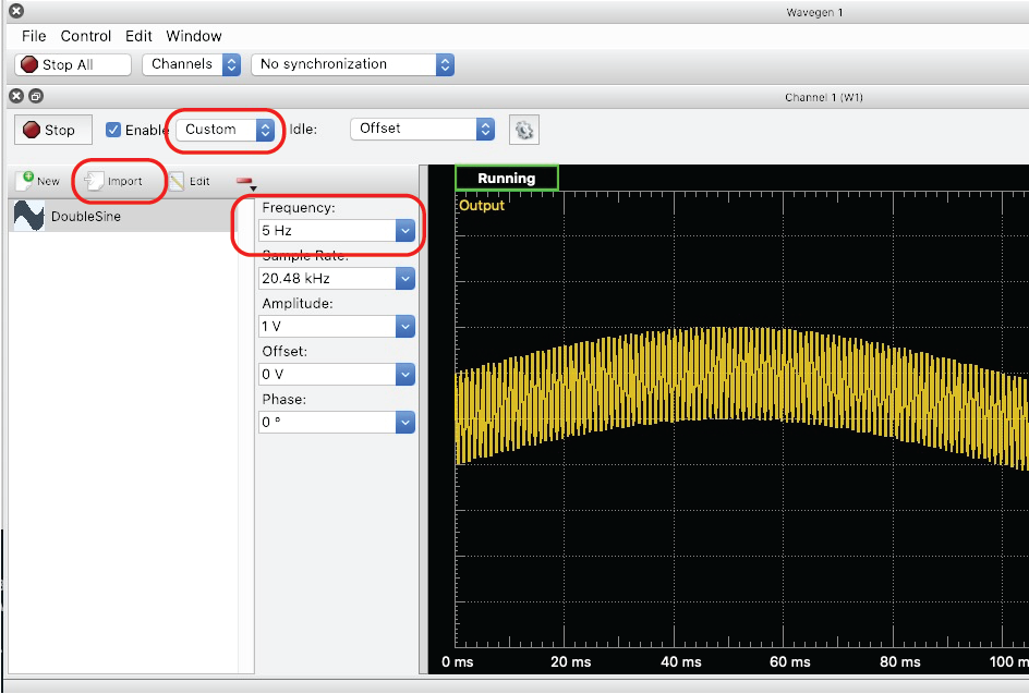
Q2.4 Can you build a circuit to filter out just the high-frequency sine? And another one to filter out the low-frequency sine? Please report how you did this (include a photo, diagram, or description in words). You might want to refer to your solution for section 3.1 of the previous assignment for inspiration.
3. Op Amp Problems
In the next few sections we will examine several circuits. First, we will look at them analytically (albeit mostly qualitatively), then you will explore their models in a web simulator, and finally, you will build the circuits on the breadboard and measure their inputs and outputs with the Analog Discovery. As a bonus at the end, you can explore the circuit models in more detail on your computer using a simulation program called SPICE.
3.1 Loop gain
Recall, that amplifier gain is defined as the ratio of the output to the input. An amplifier that takes an input voltage and produces an output voltage has voltage gain: $G_V=\frac{V_{Out}}{V_{In}}$. Consider the non-inverting amplifier shown below, a fraction of the output voltage is fed-back (via the voltage divider) to the inverting input. Internally, the amplifier attempts to maintain both inputs at the same voltage, and it does so by adjusting the output voltage.
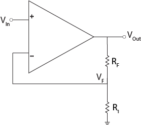
Non-inverting Amplifier
Q2.5 Compute the closed-loop gain for the non-inverting amplifier circuit. Assume that the device behaves as an ideal Op Amp – that is, no current flows into either input terminal, and the voltage at both inputs is the same.
HINT: First, use the voltage divider equation to calculate the voltage on the $V_F$ node expressed as a function of $V_{Out}$. This voltage will appear at the inverting terminal, and in response, the Op Amp will adjust its output voltage so that $V_F= V_{In}$. Next, rewrite the expression for $V_{Out}$ as a function of $V_{In}$. And finally, rearrange the terms to obtain an expression for gain.
3.2 Simulation Demos
In this section we will look at two live demos of Op Amp circuits that we explored earlier. In the demos below, voltage is represented by the color of the wire, and current is shown as the moving dots. In this simulation, the Op Amp behaves as an ideal device with zero input current. The input and output waveforms are shown in the oscilloscope trace, and resistor values can be controlled by moving the sliders on the right panel. Hovering the mouse over a waveform will display the voltage value (it’s convenient to first pause the simulation using the RUN/STOP button).
Q2.6 Please convince yourself that the non-inverting amplifier below is the same circuit as shown in the figure above. Using the gain equation you derived above, pick resistor values to achieve gain of ~2. What values did you use? What are the amplitudes of the input and output waveforms?
Q2.7 Increase the gain to 10. Explain what happens to the output waveform?
The simulation below is the inverting amplifier that we examined in class. The output is inverted (180$^\circ$ out of phase). Adjust the resistor sliders and observe the output waveform. The gain for this circuit is $G_V=-\frac{R_F}{R_{In}}$.
Q2.8 Pick resistor values to produce gain -10. What values did you use?
The input impedance of this circuit describes how much current the source must provide to maintain its voltage – here, it is just the resistor $R_{In}$. To understand why that’s the case, consider that the Op Amp maintains both inputs at the same voltage. Because the $V_+$ terminal is grounded, the $V_-$ terminal is also kept at the ground potential – this is called a “virtual ground”. The current that the source has to provide flows from the source to the virtual ground across $R_{In}$
Q2.9 The input voltage source produces a 1 V sinewave. With the resistors you chose, what is the maximum current that the source outputs?
3.3 Circuits
In the class materials, we provide you with a Texas Instruments LM324 OpAmp. We will use this microchip (also called an Integrated Circuit or IC) to build some of the simple circuits that we analyzed analytically and through simulation. This particular IC has 4 identical Op Amps inside, and you can use any of them – this is convenient when you have to build a circuit that has multiple stages, as you can do so with a single chip.
Before you place the Op Amp on the breadboard, you may need to gently bend the pins inward so that they better line up with the holes. Position the IC so that it spans across the middle divide of the breadboard. Remember, that Op Amps need to be powered. Connect power (V+) and ground, to pins 4 and 11, respectively. To identify the pins, you can refer to the image below (from page 3 of the datasheet). Also, every IC has a key, notch, bevel, or other marking, to identify pin 1. With the key at the top, pins are numbered counter-clockwise, starting with pin 1 in the upper left, but it’s always a good idea to confirm with the datasheet. Once you connect power and ground, your Op Amp board should look similar to the picture below.
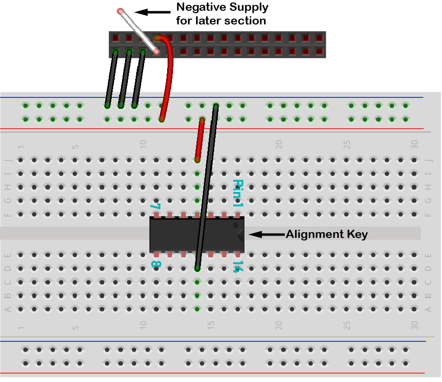
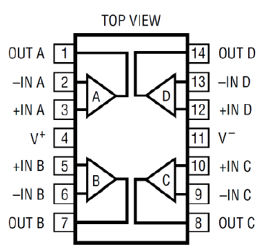
Op Amp Power Connections
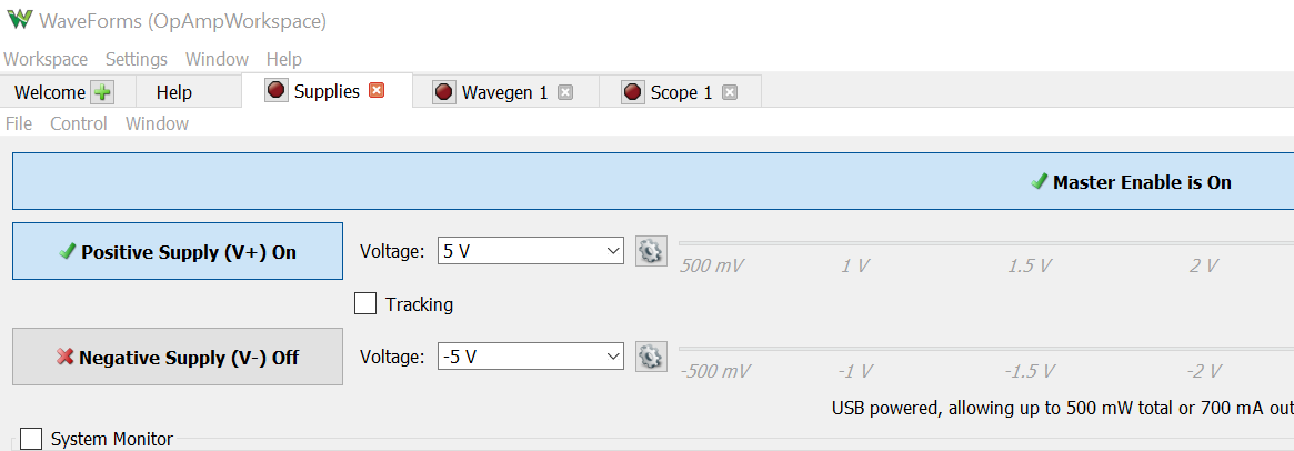
To power the Op Amp from the Analog Discovery, go to the Welcome tab and select Supplies. This will pop up a new tab, which has two supplies available. We will only use the positive supply. Set it to 5V, enable it, and turn it on by clicking the appropriate buttons, as shown below. We are now ready to build and test our first Op Amp circuit!
3.3.1 Buffer
In section 2.3 of the previous assignment we encountered a problem where the signal from a high output impedance source was attenuated when measured by the oscilloscope. This happened because the scope input formed a voltage divider with the source resistance. We can use an Op Amp circuit to convert a high impedance signal into a low impedance signal, which can then be correctly measured by the oscilloscope. A circuit like this is called a buffer or a voltage follower and is the main component in a electrophysiology pre-amplifier. The buffer circuit (described in the lecture) has an extremely high input impedance – in other words, it draws negligible current from its input source. But its output impedance is low, so it’s capable of outputting current without any voltage drop.
Make sure the power supply is turned off to avoid making accidental shorts as you assemble the circuit. Configure the Op Amp on the breadboard as a buffer by connecting the output directly to the inverting input using a jumper wire as shown in the schematic below. Refer to the IC pinout for reference.
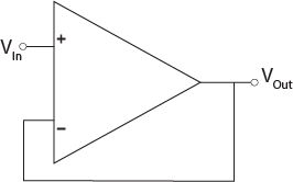

Buffer
In the wavegen tab, revert back to simple waveform and generate a 1 V sinewave on W1 and be sure to set Offset: 2V. Place a 1MΩ resistor between W1 and $V_{In}$ to produce a high impedance signal, just like you did in section 2.3 of the last assignment. Recall that previously, the signal was attenuated due to the voltage divider formed with the oscilloscope input. Turn on the power supply and measure the signal at the output of the buffer. You may need to adjust the trigger level on the oscilloscope screen to properly display the signal.
Q2.10a What amplitude do you measure at the output of the buffer? Why?
Q2.10b While continuing to measure the buffer output, connect the second channel of the oscilloscope (O2) to the buffer input $V_{In}$. What voltages do you now measure on both channels? Why?
3.3.2 Non-Inverting Amplifier
Next, you will build a non-inverting voltage amplifier. Instead of dismantling the previous circuit, use a different Op Amp on the same chip. Connect two resistors to implement the amplifier topology shown below. The exact resistor values don’t matter, but their ratio sets the gain. Recall from lecture, and from earlier in the assignment, that gain for this topology is $G_V=1+ \frac{R_F}{R_1}$. Aim to achieve gain between 2 and 10, and use resistor values 1kΩ$<R<$1MΩ.
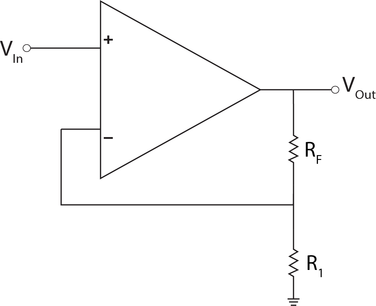

Non-Inverting Amplifier
After your circuit is assembled on the breadboard, produce a 200 mV sinusoid with a 250 mV offset from the Wavegen tab and connect that signal to $V_{In}$ of the circuit. Examine the output on the oscilloscope, does it make sense? Notice that the circuit amplifies both the DC offset and the sinusoid.
Q2.11 Based on the resistors you chose, how much voltage amplification do you expect to see?
Q2.12 Apply a zero-mean 200 mV sinewave to the input of your circuit byt setting Offset: 0V. What does the output look like? Can you explain why? Does this match your prediction from above?
3.4 BONUS
If you have time and are interested in exploring these topics further, we give a few options below.
3.4.1 Voltage Reduction
Build an inverting amplifier circuit, and choose resistors $R_F$ and $R_{In}$ to produce gain of -1/2. This is useful for reducing signal amplitude, while maintaining low output impedance – e.g. you may need to do this if you have a 5V analog source and a 3.3V digitizer. By comparison, gain<1 can’t be achieved with a non-inverting amplifier.
3.4.2 Adjustable DC Offset
You can introduce a DC offset by adjusting the voltage on the non-inverting terminal $V_+$. Instead of connecting it to ground, wire it up to the center pin of a potentiometer. Connect the other two pins of the pot to 5V and ground.
3.4.3 Falstad Demos
There are numerous interactive demos like the ones shown earlier in the assignment. Feel free explore other topics. You can open other pre-made circuits from the Circuits menu. In particular, Circuits\Op-Amps\Amplifiers lists some of the basic circuits introduced in this class.
3.4.2 SPICE Models
SPICE is an industry standard set of circuit simulation tools. The acronym stands for Simulation Program with Integrated Circuit Emphasis, and there are several versions available from different vendors. One of the benefits of using SPICE, is that it has detailed models for specific components. For example, you can find a model for the exact Op Amp you plan to use in a circuit. These models include many non-linear and non-ideal effects often seen in real circuits.
Download and install LTspice from Analog Devices and download the SPICE demo file from the class webpage. The demo file contains circuits that were presented in lecture. Run the simulation by selecting /Simulate/Run from the menu, or by clicking the ( ) icon in the toolbar. Once the simulation successfully completes (this should only take a few seconds), a new window will pop up that can display various waveforms. You can invoke a voltage probe by hovering the mouse over a circuit node (such as a wire) in the schematic window. Once you click on a node, the voltage waveform at that node will be plotted.
Hovering the mouse over a resistor will present a current probe, and clicking on the resistor will plot the current through it. Work through the examples by plotting input and output waveforms for the four basic circuits in the demo. Do they make sense to you?
Resistor value can be changed by right-clicking on the resistor. Examine the non-inverting and inverting circuits. Modify R1, R2 and R3, R4 to adjust the circuit gain for these two topologies, respectively. Plot the input and output waveforms. Did the plots change as you expected them after adjusting resistance values?
Parts List
Parts from assignment 1 plus:
- OpAmp chip (LM324)
- Aluminum foil
- Short alligator cable(s)